Retro & Vintage Computers and Appliances
The AAPRO XTIDE Card
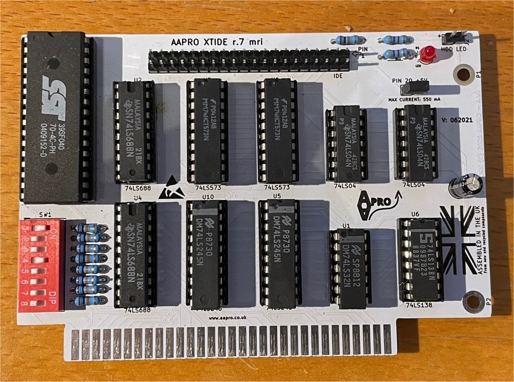
The following is a review and overview of an undocumented XTIDE clone PCB labelled "AAPRO XTIDE r.7 mri" I bought on Ebay.
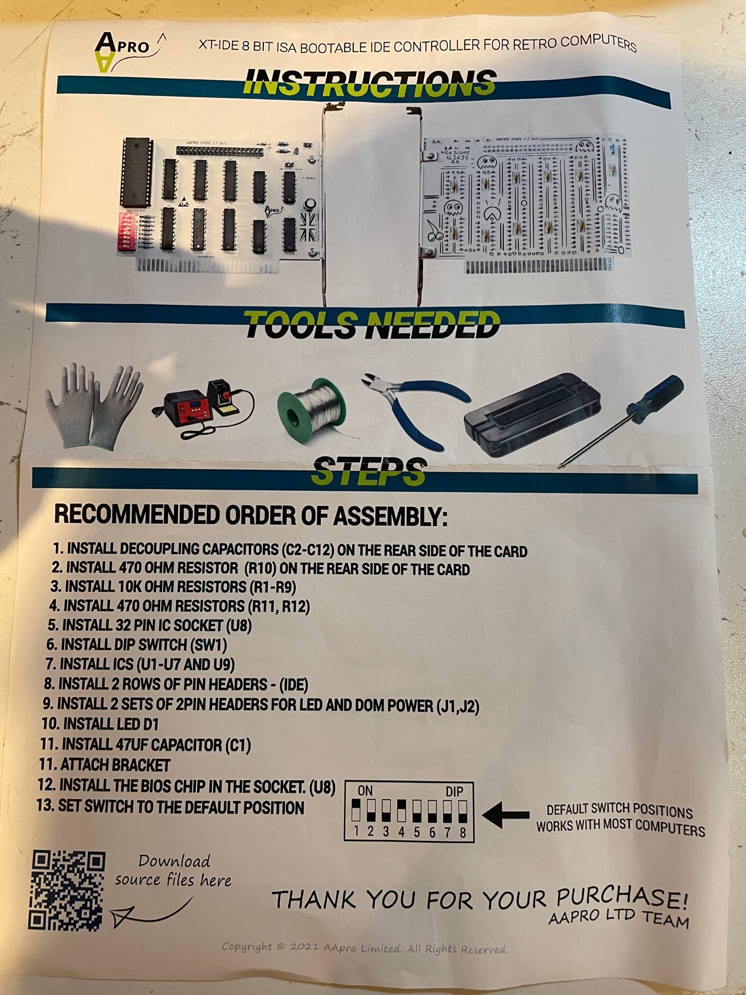
When I originally searched to buy an XTIDE board I discovered the choice from UK sellers was very limited. Having never used one before, rather than buy from an international seller, I bought what was at the time the only PCB I could find in stock from a UK seller. This came with just the PCB, bracket and a pre-programmed EEPROM which was covered with a sticker hiding the EEPROM type. I expected this board to be the same or very similar to the other well-known open source designs, however it turned out to be substantially different and almost completely undocumented with no schematics provided with the card and absolutely no technical information (not even DIP switch settings) on the seller's website. The only info provided was an A4 piece of paper containing a "recommended order of assembly" and two stickers on the box lid, one a brief component list (which did not even list the EEPROM type) and the other the DIP switch settings. These labels tore when I tried to remove them to throw away the box (I very nearly threw them away with the box)!UPDATE 2022-07-24:
A month after I had basically given up on the AAPRO board and after I had already written this page, I took another look at the supplied A4 sheet of paper in order to upload it to this site. For the first time I noticed that at the bottom there's a QR code and the words "Download source files here" next to it. No actual URL or anything, just a small QR code that looks like part of the artwork. After installing a QR code reader app and scanning this with a phone, this reveals a hidden website address of https://appgal.aapro.co.uk/xtide/ which was not linked from their main www.aapro.co.uk site and didn't come up when searching. This obscure site contains the open-source hardware and firmware images they are legally required to provide, but in what seems to be the most user hostile way imaginable. My mind is utterly and totally boggled as to why they would not provide any support or tech info on their website for their products and customers, or even documentation with the product, but instead would bury it in a mysterious QR code on a piece of paper that appears to be designed to be thrown away. I can only conclude that a locked filing cabinet in a basement room labelled "beware of the leopard" was considered too obvious. I've mirrored the files here to make them easier to find.
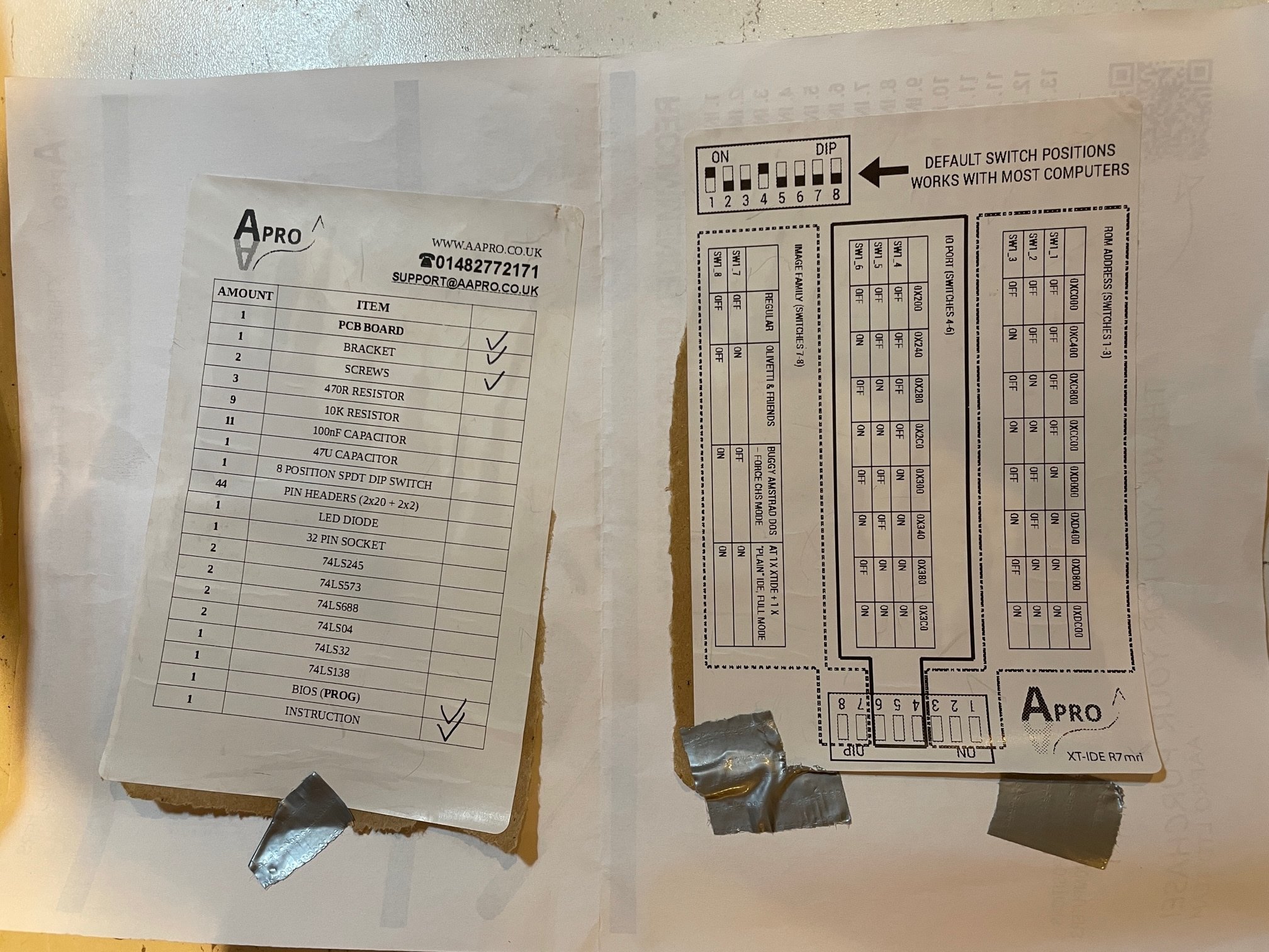
This is the entirety of the documentation provided with the card including the two stickers from the inside lid of the shipping box:
The Review
It didn't start well. I ordered the card and within a week they send me a kit for an Adlib sound card! To give them credit I contacted them and they sent a return label the same day and promptly sent the correct item as soon as they received the wrong one back, so no major delay in actually receiving the item compared to some other Ebay sellers, but a substantial hassle in having to go to the post office in the middle of the day to fix their mistake. But these things happen, so I wasn't concerned as their communication was good, though it was clearly foreshadowing.Once the correct item was delivered, I started to build it. The board appeared to have absolutely no quality control whatsoever, with multiple holes blocked by solder mask and given how hard it was to remove, metal or solder under it. This required drilling of five holes causing slight damage to the board in order to fix. I've not seen this issue on boards made this century despite having ordered my own from China many times. I can only imagine it's either an issue with the type of solder mask, or the boards were made by the absolute cheapest manufacturer without quality checks.
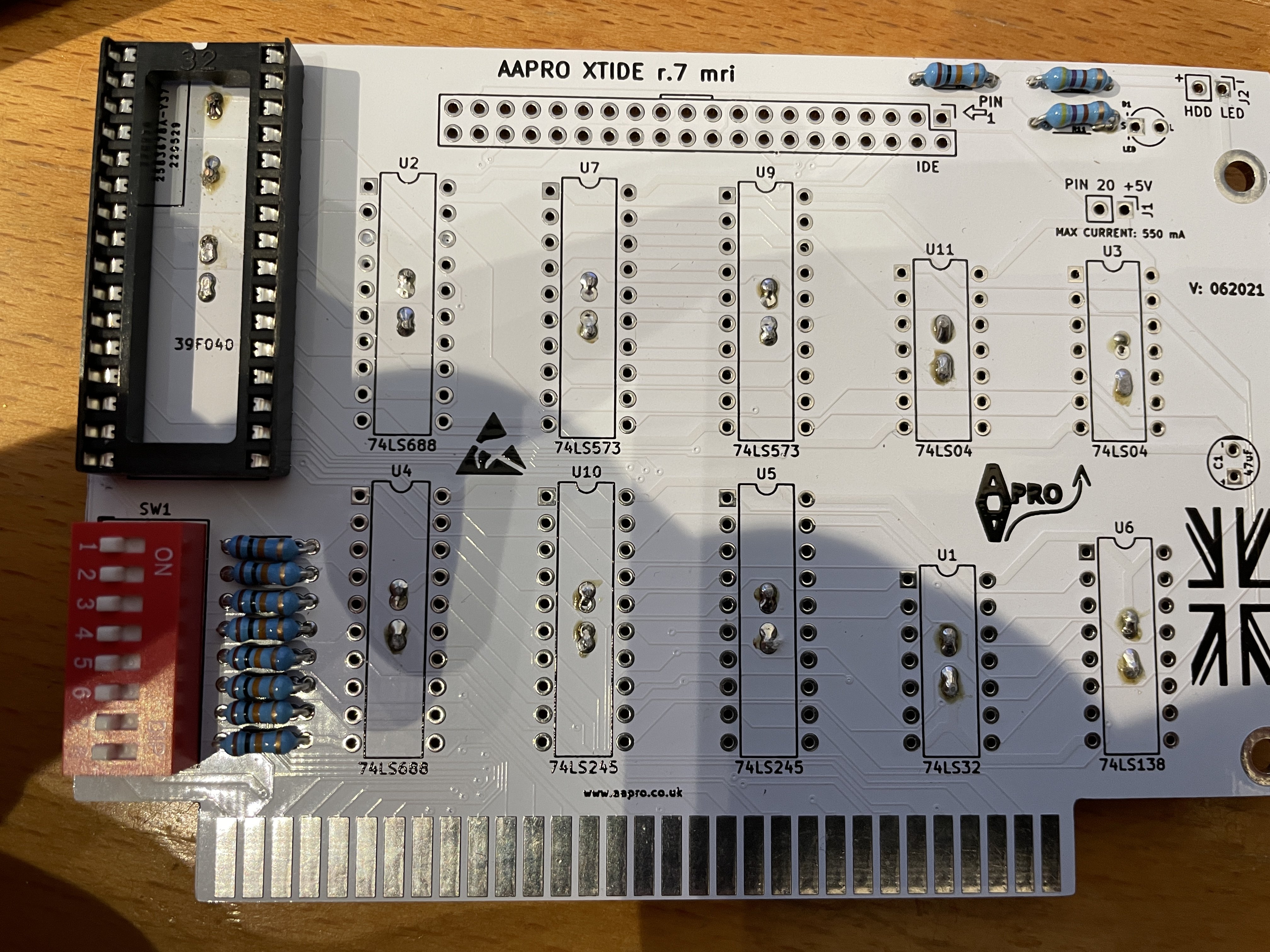
The board after drilling out some blocked holes to fit caps. U2 still has two blocked holes and has to go on top!
The way they've designed the board, some components (such as decoupling capacitors) have to be soldered on one side of the PCB before the IC sockets can be soldered over them on the other side. This means the IC sockets have to be soldered after the decoupling caps and if there's any issue with either, desoldering both may be required. Of course the blocked holes were on a capacitor and a couple of IC sockets, in exactly those locations, making it likely I would need to desolder one or two sockets to fix any issues caused by the blocked holes.
To make matters worse, the whole board is coated in a white solder mask that almost completely hides the traces (there's no schematic remember) making tracing out the circuit to fix check this an absolute nightmare. Just to rub salt into the wound, they've printed Pacman style characters on the rear of the board (where the decoupling caps are) just to add to the confusion.
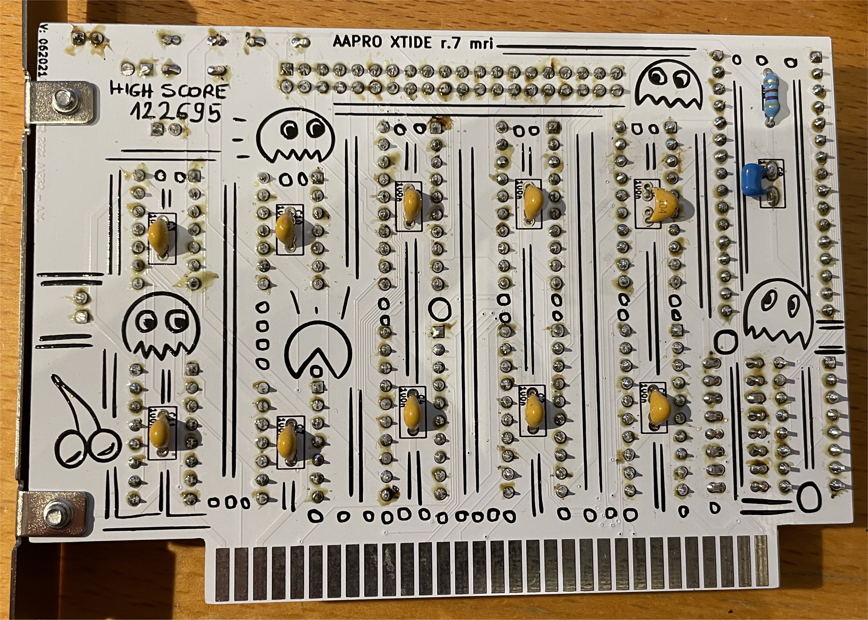
The PCB before cleaning so you can see the white solder mask in context.
If these blocked holes had also been vias (in fact they may have been - I never managed to fully trace out the circuit) and not soldered on both sides, they could have been broken by needing to be drilled and that would have been extremely hard to troubleshoot due to the placement of the decoupling capacitors, the white solder mask and the complete lack of documentation. In addition, no schematic, no circuit diagram and no component placement layout (other than that printed on the PCB itself and obscured both by the components themselves and from the need to repair the manufacturing defects) were provided.
The confusing graphics and traces obscured by solder mask, also means the markings that do exist on the PCB are the only indication of what component should go where and some of these markings (including all the resistor values) are obscured once the components are installed, again pointlessly making fault finding harder. I even struggled to identify which holes for the activity LED were anode and cathode. Almost none of this would have been an issue if a component layout or schematic was provided or available on their website. The blocked holes and lack of documentation also became a serious issue when I wanted to add a power connector for an IDE CF adaptor and could not easily confirm where the traces on the board went. A few days after building the board I realised that one of the pin headers enabled 5v on IDE pin 20 (since this was my first XTIDE board I didn't know about pin 20 power when building it so thought the ambiguous jumper label meant it was a 5v source to connect a cable). Without knowing that I could easily have short circuited the computer power supply if I'd used a CF adaptor or drive without power on pin 20 support, but in the end it just caused me to made an unnecessary power cable as I did have pin 20 support. I wonder how many people's computers may have been damaged because of that lack of documentation.
Once built, the only place the DIP switch settings are written is on a sticker fixed to the inside lid of the packing box, which could easily have been thrown away by that point. Not on the provided single piece of single sided A4 paper that tried to give the appearance of instructions, not on the PCB (no that was full of silly Pacman characters so no space for any useful info), not on their website or online anywhere. The label inside the box lid was firmly stuck, so I had to tear the carboard to keep it! This is utterly unacceptable, as in a few years these cards might be found in PCs with no ability for the new owners to configure them or fix any issues.
Since there was no detailed bill of materials there was also no list of possible substitutions, which given that this board required the customer to source every component other than the EEPROM and a bracket, seems ridiculous. The chips used are mostly the same as other XTIDE cards, so I took a chance that other 5V equivalents (LS, ALS, ACT, or HCT) listed for another XTIDE card would work and they did, but by that point I was very much wishing I had bought the other card.
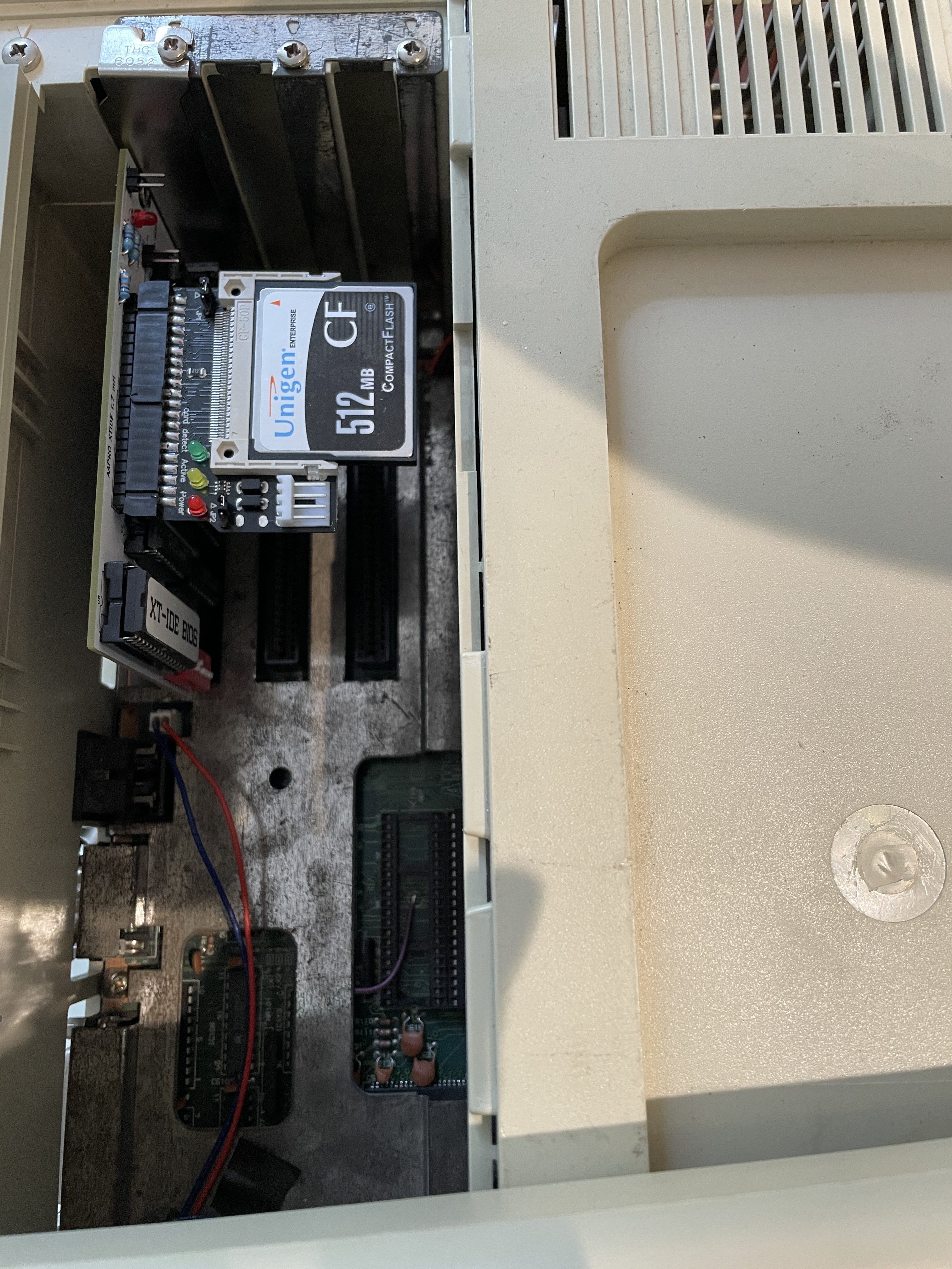
Once built it actually worked, then I realised the biggest issue with the board, the one that made it unusable for me. The IDE edge connector is at the top, not the rear or front of the card, meaning that an IDE to CF adaptor cannot be directly plugged in without an extension cable in almost all cases, as it obstructs other cards or would be obstructed by the case.
It's not as if I would have wanted to use those slots for an Adlib card. :-)
Did I mention that the EEPROM they're using is a 32 pin 39F040 which is very different from the 28 pin 28C256 and 28C64B used by other cards. It's unclear if this can be flashed with the usual XTIDE utilities (they don't have an option for that EEPROM) so I've not tried as I don't want to risk bricking the card, but again this could be so trivially solved with documentation.
Final minor items for comedy value: Despite being a blank PCB assembled by the customer, it had "Assembled in the UK" printed on it. I guess that's ok if all their customers live in the UK and build the boards there, but how do their know? It's also at a minimum rather contentious if you happen to build the device in Northern Ireland. Elsewhere in the world it would be an actual lie and require covering over if the board was to be resold. A company shouldn't try and claim national ownership of assembly work done in another country.
I've made a bin file of the EEPROM chip from my board which can be downloaded here for anyone who does brick their board.
I very quickly realised that the location of the pinout alone on this board was a show stopper, so decided to move on and build a properly documented and fully legally compliant open source replacement XTIDE card that could be assembled and repaired without being dependent a single seemingly customer hostile company.